Semicon equipment and metrology
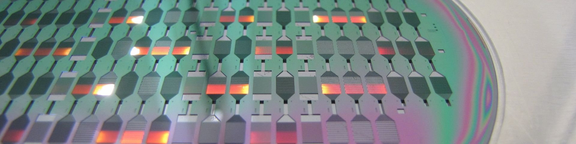
The manufacture of semiconductor chips requires extreme precision on a nanometre scale. Ensuring consistent quality and mitigating contamination during manufacture calls for metrology solutions that can accurately measure each step in the process. TNO Semicon equipment and metrology provides novel or improved metrology solutions for the entire semiconductor ecosystem and related industries.
Quality chips for all
Semiconductor chips and devices are an integral part of our digital world. And as those chips and devices decrease in size and increase in capacity and computing power, the need for precision, accuracy, and contamination-free production increases. TNO partners with stakeholders throughout the value chain to provide assurance of quality and accuracy in chip development through advanced metrology solutions. We work with chip manufacturers and validate and demonstrate metrology equipment concepts for other high-tech industries in, amongst others, the space, nuclear, and quantum technology domains.
Chip production occurs on the edge of what is technologically possible, and optimising that production requires a multidisciplinary approach. To enable continuous advancement in semiconductor technology, our experts offer:
- device process management
- metrology solutions
- novel or improved components and equipment
- experimental setups (both in laboratory and industrial settings)
Our unique expertise in ultra-clean vacuum technology, Atomic Force Microscopy (AFM) metrology, computational physics, plasma physics, heat, mass and flow transfer, particle contamination, lifetime, state-of-the-art setups, and systems engineering enable us to provide the most effective solutions for the industry’s biggest challenges.
Front-end optimisation
For more than 25 years, TNO has partnered with ASML and its suppliers to optimise lithography equipment and ensure optimal performance. As companies search for ways to make more complex chips, faster and more accurately than ever, TNO Semicon equipment and metrology researches and also develops ways to modify older machines or create new components that can accommodate that demand. With a particular focus on preventing contamination and assuring precision production, we work with ASML and its suppliers to develop the metrology systems that can accommodate modern demand.
Back-end acceleration
After a wafer is patterned, semiconductor manufacturers conduct their unique and proprietary production process, including cutting, stacking, interconnecting, packaging, and more. Here, too, precision and prevention of contamination are paramount. We research, develop, and help to realise solutions that ensure each chip is manufactured with the desired accuracy under contamination-free conditions, at the speed and volume that industry demands.
Chip manufacturers, equipment and component suppliers, and other high-tech industry stakeholders in the semiconductor value chain rely on us to solve their most complex production challenges. Our multidisciplinary team is ready to work to solve yours as well. If you would like to uncover ways to improve or refine your production process with contamination control and/or precision metrology, contact us today.
Heat flux profiler
In a lithography machine, measuring and controlling heat and heat flux is essential, and yet also a significant challenge. TNO Semicon equipment and metrology develops sensor technology to determine heat flux with proprietary ASML equipment in our own labs, and designs solutions to constantly improve equipment or components for better heat flux control.
Atomic force microscopes
TNO’s nanophysicists make use of atomic force microscopes and infrared atomic force microscopes to measure chip surface structures at near-atomic levels. Based on those measurements, we are able to make the most advanced improvements to wafer quality and keep up with the growing demand for even more complex and powerful chips produced at an even faster pace.
Contact us
-

Frank Driessen
Functie:Research manager Semicon equipment and metrology-
Standplaats:Delft - Stieltjesweg
-
Email:Email Frank
-
Get inspired
Quantum internet and quantum networks series 1.0

TNO and Quobly join forces to advance industrial-scale silicon quantum technology

TNO Semicon Event 2026: Building bridges to reach Moore
Pioneering with a purpose: The Netherlands at the forefront of quantum innovation
Pioneering on the edge of physics: quantum chips tested faster and faster
