Quantum devices and materials
Important performance indicators for quantum devices can be traced back to chip design, material quality and defect density. In addition, nano- and micro-fabrication are crucial, as quantum states are fragile and need protection from a noisy environment. TNO offers expertise and support at every stage of material and quantum device development. From design and modelling to fabrication and characterisation to standardisation, we provide the expertise and facilities to drive quantum innovation.
Expertise that drives innovation
As a co-founder of QuTech in 2014, TNO developed critical knowledge and experience in the design, fabrication, and characterisation of quantum materials and devices. A wide range of patents and publications showcase our various in-depth competencies, innovations and achievements. Today, we put that expertise to work to drive innovation and accelerate the development of revolutionary quantum technology.
Our primary goal is to partner with both small and large companies to enable an increase in the TRL level of their innovations and help these enterprises overcome the infamous valley of death. In addition, we also contribute to key European consortia, such as Qu-Test & Qu-Pilot, ARCTIC, and QLSI2, which aim to develop critical knowledge and competencies that drive the entire quantum industry forward.
Characterisation that accelerates
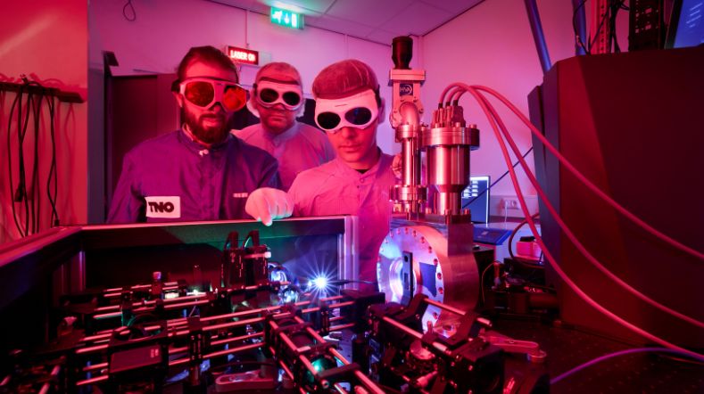
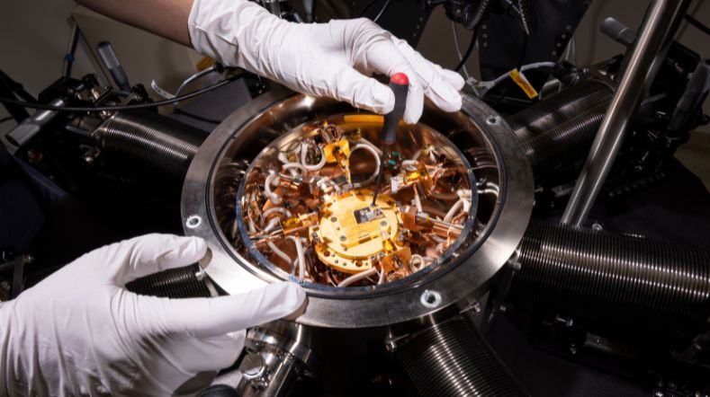
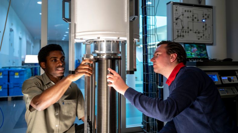
Among the array of services we provide, our in-depth device characterisation and metrology capabilities fill an important – and often unmet – industry need. We provide an on-demand, high-throughput test-bed for device screening and in-depth material and device characterisation. This enables a better understanding of device fabrication yield, reproducibility, and other device parameters. In this way, QPU manufacturers, QPU designers, and full stack integrators can validate the quality of their devices and materials, and also make use of our fast feedback loop to make rapid improvements to device design and ensure accelerated development. Our test lab, QITT, supports the quantum ecosystem and ensures constant growth in knowledge, experience and capabilities.
QITT
QITT is one of the few highly competent quantum material and device characterisation facilities in Europe. It acts as an enabling facility for various critical B2B and EU projects in which TNO is a key stakeholder. It provides state-of-the-art infrastructure and an array of device screening, as well as in-depth device/material characterisation capabilities, to organisations of all sizes around the world. In addition to fostering B2B and EU collaborations, the facility enables faster feedback to design teams, which accelerates device development and prototyping.
High-quality design and fabrication
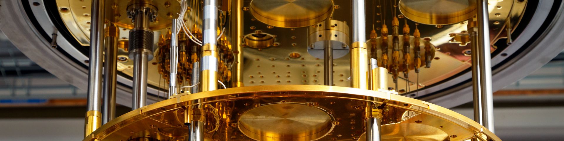
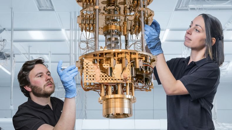
TNO also contributes to device and chip design, in particular for spin qubit devices and superconducting quantum devices. Together with our clients, we also conduct on-demand fabrication of Si/Ge quantum dot devices, quantum devices in diamond, and superconducting quantum devices. All fabricated devices undergo precise characterisation and validation at our facilities. We consult on the development of specific quantum device prototypes and on advanced fabrication processes. The knowledge and expertise we acquire in these processes informs our work moving forward.
About our fabrication facilities
TNO’s Van Leeuwenhoek Laboratory (VLL) cleanroom is the site of state-of-the-art equipment for material etching and deposition, lithography, material growth, and more. Here, TNO experts specialise in the nanofabrication of Si/Ge quantum dot devices, super- and semi-conducting hybrid devices, superconducting quantum devices and quantum devices based on color centers in diamonds. And, of course, the microscopic and optical inspection of these devices and materials.
Materials research and support
TNO’s deep understanding of material defects is crucial for improving chip design and understanding device behaviour. TNO offers its expertise in materials and metrology of material properties to better understand device performance and reduce noise. We also offer expertise in the design and fabrication of test structures for material analysis. We have both the knowledge and facilities to optimise this crucial component of device development and optimisation.
Preparing for the next wave
The quantum revolution is upon us. And TNO is eager to contribute to its acceleration in as many ways as possible. We are ready to apply our expertise and facilities to support the industry and be a trusted partner in device and material development. Contact us today to explore the possibilities.
Contact us
-

Saurabh Karwal
Functie:Business Developer Quantum Technology-
Standplaats:Delft - Stieltjesweg
-
Email:Email Saurabh
-
Get inspired
TNO expands quantum information technology testing capabilities to support startups
TU Delft appoints TNO’s Richard Versluis as Quantum and Computer Engineering Fellow
Quantum communication systems

Quantum computing
TNO delivers Germany’s first quantum internet node