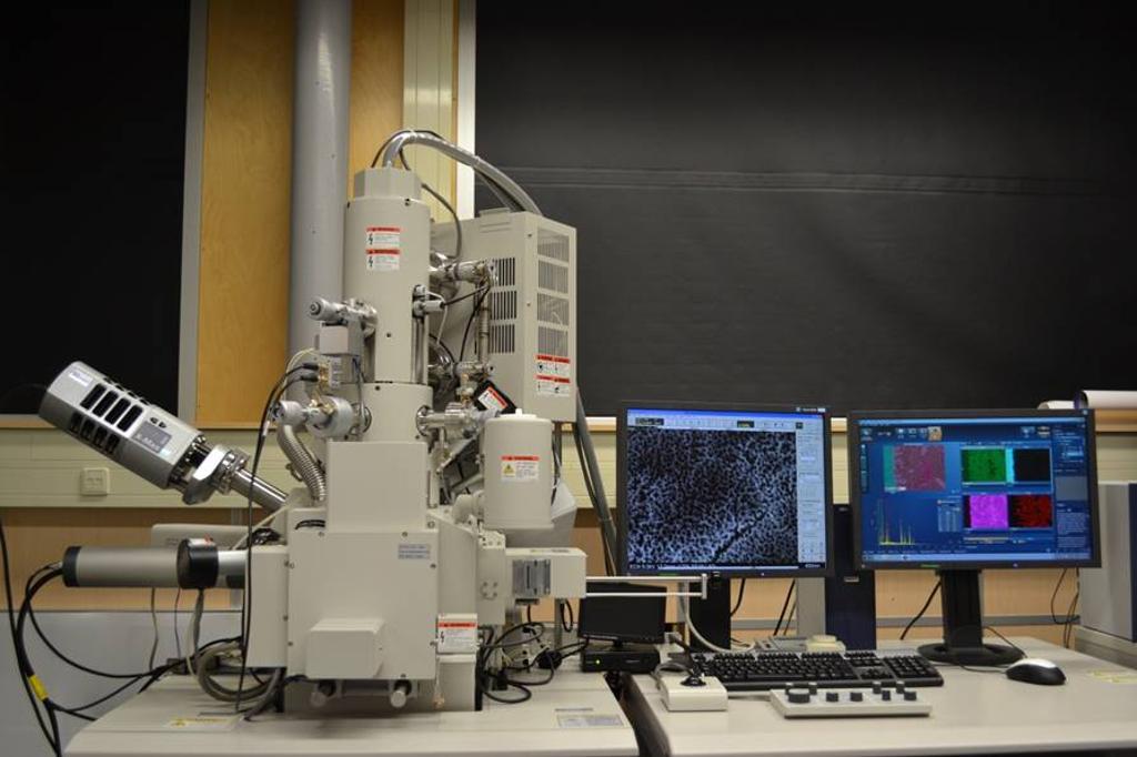
Hitachi SEM SU-70
- Category:
- To be determined
- Brand:
- Hitachi
- Type:
- SU-70

Description
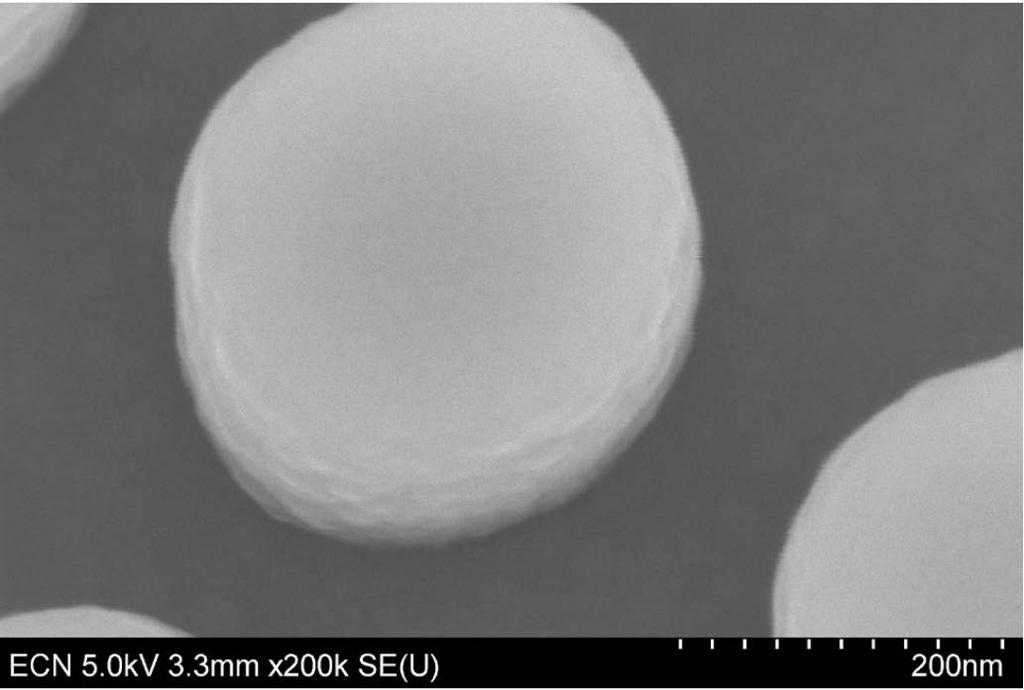
The Hitachi SU70 is a so-called Schottky FEG Scanning Electron Microscope. It is primarily used with materials science research. The electron source also allows non-conductive materials, such as alumina, to be examined to a resolution of about 3nm without applying a conductive layer. Such a layer covers small surface details.
In combination with ion milling, thin layers as small as 3-4nm can be characterised.
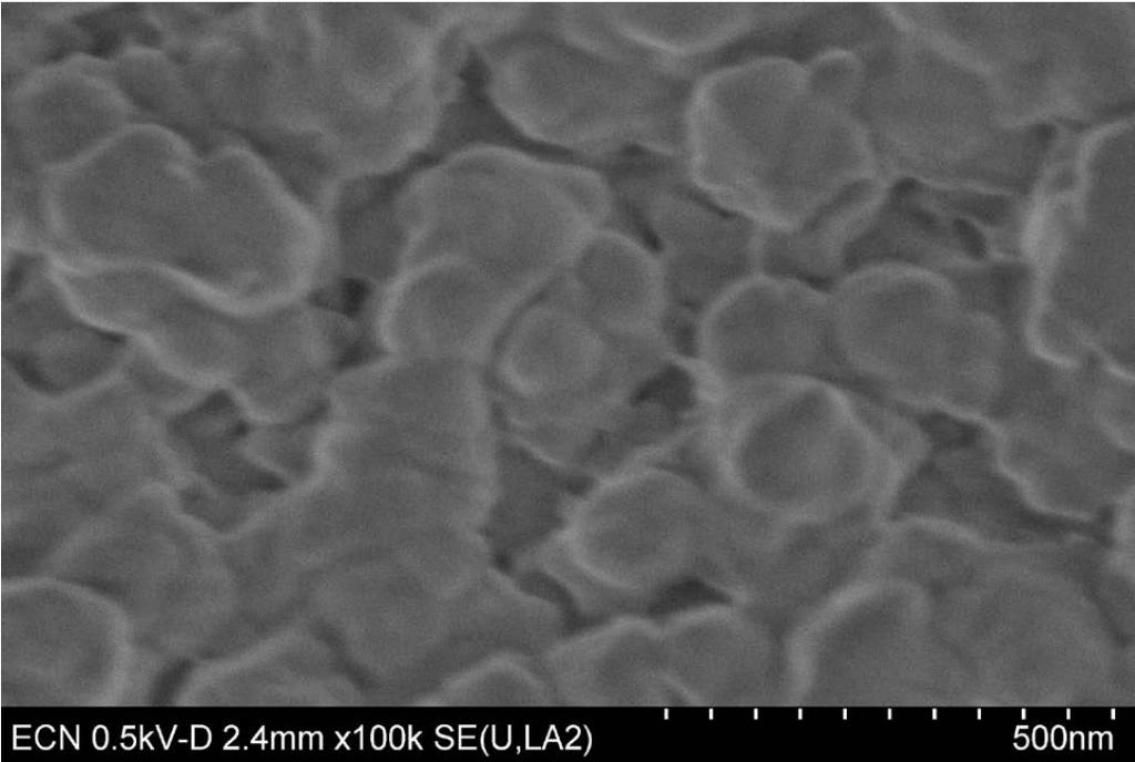
By using a so-called top detector, back-scatter electron images at low acceleration voltages (e.g. 2kV) can be made. This improves characterisation of surfaces.
Technical details
Sample size, maximum: round 150mm and up to 25mm high
Sample tilt (for EBSD) up to 70°
Field-free lens mode for EBSD
Tilt: -10°/+70°
Deceleration mode: for very low landing energy for research on beam-sensitive or poorly conductive materials
Semi-inlens mode with Super ExB filter
BSE detector with 5 segments, allowing the creation of a BSE-3D image.
Resolution: better than 0.9nm at 30keV, 1.6nm at 1keV under optimal conditions.
Accelerator voltage from 0.1keV with nm resolution
EDS element analysis from Bore (B)
High vacuum
High and very low beam currents, for optimal choice between surface examination at high resolution and material analysis
Additional techniques
EDS, Energy Dispersive Spectral Element Analysis
WDS, Wavelength Dispersive Spectral Element Analysis
EBSD, Electon Beam Scattering Diffraction
BSE, Back Scatter Electron
Applications
Examples of applications:
Research catalysts and electrolysers
Damage assessment
Material analyses, chemical composition
PMI (Positive Material Identification)
Texture research
Crystallography
Corrosion testing
Tribology and wear testing
Surface examination of non-conductive materials such as aluminium oxide
For other applications, feel free to ask a question

