Ion Milling System
- Category:
- To be determined
- Brand:
- Hitachi
- Type:
- IN4000

Description
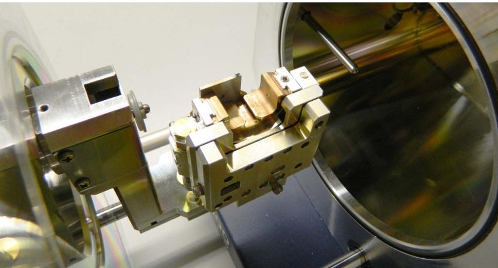
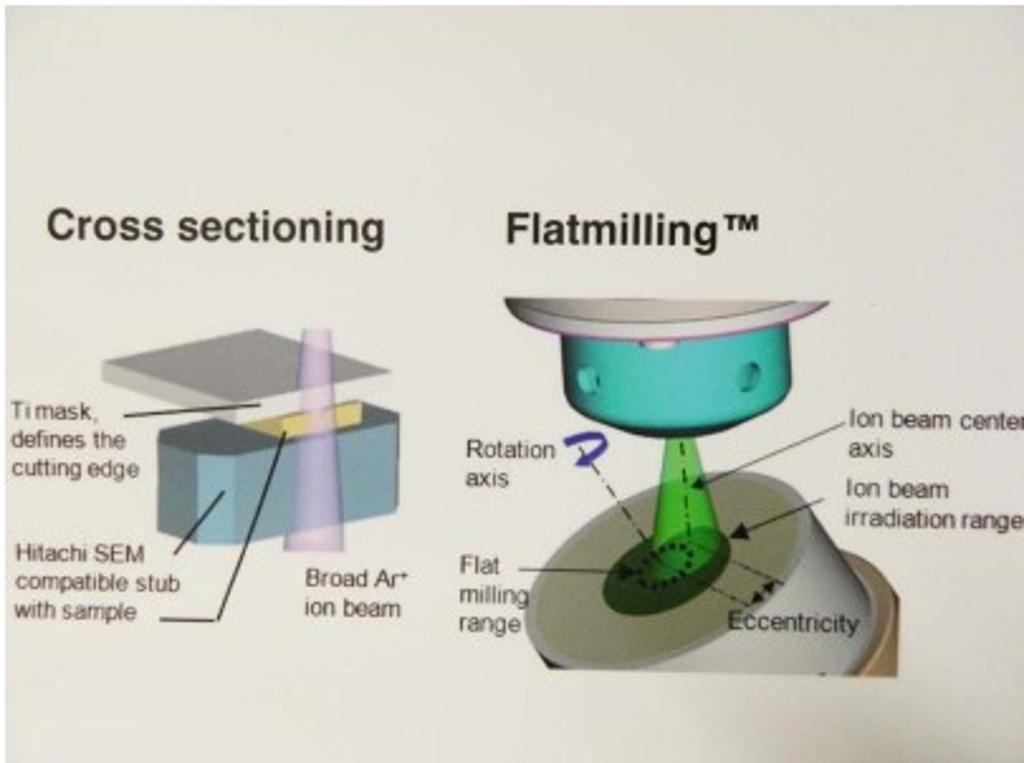
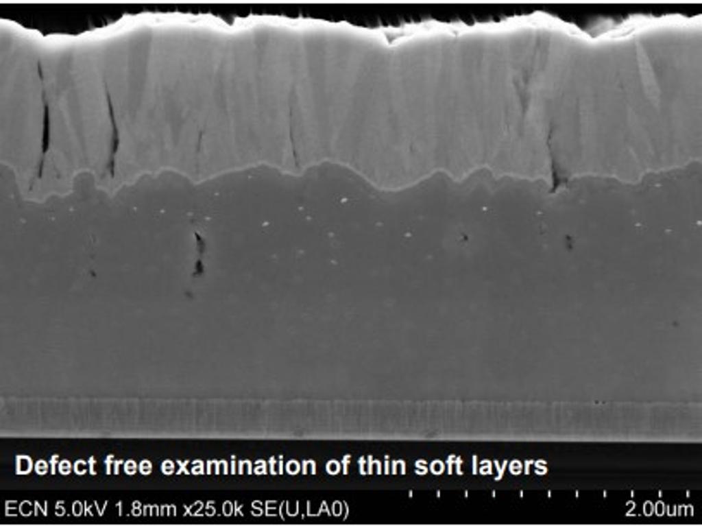
An Ar plasma beam is used to create cross sections of thin sections or layers, typically up to 500µm. The thickness is limited from economic and machining time considerations. During machining, a deformation-free surface is created. Ideally suited for research on cross sections of thin layers (from 2-3nm). Think of atomic layer deposition (ALD). Surfaces of cross-sections can also be polished (flat milling) where several nano-metres of material is removed. Suitable for making deformation-free surfaces for e.g. EBSD (Electron Beam Scattering Diffraction) analysis.
The machined surface is heated to about 80°C. This may somewhat limit the application on heat-sensitive materials.
Technical details
Sample dimensions: LxWxH - 20x10x5 mm
Section width: 1-2mm
Processing time depending on sample material and thickness: 10 min to 2 hours
Positioning: standard down to 10µm, possible down to 1µm.
Maximum sample surface temperature approx. 80°C
Cross-sectioning and surface polishing of metallographic sections
Materials: all. Limitations for heat-sensitive materials
Additional techniques
Scanning electron microscopy
EDS and WDS element analysis
EBSD: crystallographic characterisation using Electron Beam Scattering Diffraction
Applications
Cross sections of thin layers (starting at about 2 nm)
Pre-processing for EBSD (electron Beam Scattering Diffraction) analyses
Cleaning of surfaces: removal of oxidation for examination
Removal of final mechanical deformations after metallographic preparation of cross sections
Characterisation of thin layers or materials prone to smearing during mechanical preparation

